Small Steps to Big breakthroughs
Tian Research Lab


Research
Overview of Our Research

Our research focuses on both fundamental studies and technological applications of solid-state (electronic and spintronic) devices based on novel quantum materials. General areas of our study include quantum (charge, spin & thermal) transport in novel quantum materials where strong interactions lead to exotic states of matter and novel electronic behavior for new device applications in nanoelectronics spintronics, future computing, and energy harvesting. Systems that we study include 2D materials (such as topological superconductors, 2D magnetic materials, topological materials, etc) and their heterostructures. We explore these systems by combining material growth, characterization, and transport studies with a variety of experimental techniques, including applied magnetic fields, electrostatic fields, and temperatures ranging from room temperature down to mK.
Below please find some broad research topics being studied in our lab as well as the highlights of our previous work.
1. Quantum Physics & Transport (Charge, Spin, and Thermal) in Low Dimensional Structures.
1) Charge transport in novel nanostructures subjected to ultra-low temperature and high magnetic fields.
2) Spin transport in 2D materials (topological superconductors, magnetic materials, 3DTIs, graphene, TMDs, ...) featuring strong or weak spin-orbit interaction.
3) Thermoelectric properties of novel 2D materials and their heterostructures.
2. Quantum Devices and Nanofabrication Techniques.
1) Developing various nanofabrication techniques.
2) Fabricating novel quantum devices for nanoelectronics, spintronics, and thermoelectrics.
3. Quantum Materials: Growth of Novel 1D and 2D Materials.
1) Growing quantum materials, such as graphene, topological insulators, 2D magnetic materials, and TDMs, ...
2) Stacking novel van der Waals Heterostructures using dry transfer techniques.
Highlights:

7. Suppressing critical current noise by an atomically thin boron nitride (h-BN) layer
Decoherence in quantum bits (qubits) is a major challenge for realizing scalable quantum computing. One of the primary causes of decoherence in qubits and quantum circuits based on superconducting Josephson junctions is the critical current fluctuation. Many efforts have been devoted to suppressing the critical current fluctuation in Josephson junctions. Nonetheless, the efforts have been hindered by the defect-induced trapping states in oxide-based tunnel barriers and the interfaces with superconductors in the traditional Josephson junctions. Motivated by this, along with the recent demonstration of 2D insulator h-BN with exceptional crystallinity and low defect density, we fabricated a vertical NbSe2/h-BN/Nb Josephson junction consisting of a bottom NbSe2 superconductor thin layer and a top Nb superconductor spaced by an atomically thin h-BN layer. We further characterized the superconducting current and voltage (I–V) relationships and Fraunhofer pattern of the NbSe2/h-BN/Nb junction. Notably, we demonstrated the critical current noise (1/f noise power) in the h-BN-based Josephson device is at least a factor of four lower than that of the previously studied aluminum oxide-based Josephson junctions. Our work offers a strong promise of h-BN as a novel tunnel barrier for high-quality Josephson junctions and qubit applications. (Journal of Physics: Condensed Matter, 33, 495301 (2021))

6. 2D 2M-WS2 Nanolayers for Superconductivity.
In this work, we report a new route to grow high-quality 2M-WS2 single crystals and the observation of superconductivity in its thin layers. The crystal structure of the as-grown 2M-WS2 crystals was determined by X-ray diffraction (XRD) and scanning tunneling microscopy (STM). The chemical composition of the 2M-WS2 crystals was determined by energy-dispersive X-ray spectroscopy (EDS) analysis. At 77 K, we observed the spatial variation of the local tunneling conductance (dI/dV) of the 2M-WS2 thin flakes by scanning tunneling spectroscopy (STS). Our low-temperature transport measurements demonstrate clear signatures of superconductivity of a 25 nm-thick 2M-WS2 flake with a critical temperature (TC) of ∼8.5 K and an upper critical field of ∼2.5 T at T = 1.5 K. Our work may pave new opportunities in studying the topological superconductivity at the atomic scale in simple 2D TMD materials. (ACS Omega 6, 2966 (2021).
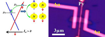
5. Topological insulator Spin "battery" for spintronics and quantum computing.
We report spin potentiometric measurements in TIs that have revealed a long-lived persistent electron spin polarization even at zero current. Unaffected by a small bias current and persisting for several days at low temperature, the spin polarization can be induced and reversed by a large “writing” current applied for an extended time. Such an electrically controlled persistent spin polarization with unprecedented long lifetime could enable a rechargeable spin battery and rewritable spin memory for potential applications in spintronics and quantum information (Science Advances 3, e1602531 (2017)).

4. Quantum transport (charge and spin) studies in 3D topological insulators.
1) We performed the systematic study of temperature and gate dependent magnetotransport, including both the weak antilocalization (WAL) and linear magnetoresistance (LMR) effects in MBE TI BiSbTe thin films grown on high-k SrTiO3 substrates. Our results showed the clearest gate-tuned bulk metal to insulator transition in TI thin films reported up to then. We found that LMR commonly observed in TI is more subtle and complicated. It can arise from a classical origin (related to disorder and inhomogeneity, sometimes called “Parish-Littlewood LMR” and also observed in many non-TI-based semiconductors) rather than the quantum LMR (sometimes called “Abrikosov LMR”) associated with Dirac fermions of topological surface states assumed in most previous studies of LMR in TIs. (Sci. Rep. 4, 4859 (2014)).
2) We performed spin potential measurements on bulk insulating Bi2Te2Se TI thin flakes and obtained the highest current-induced spin polarization reported so far. (Sci. Rep. 5, 14293 (2015), Nat. Commun. 10, 1461 (2019)).
3) We demonstrated the electrical injection of a helically spin-polarized current into graphene through a 3D TI thin flake as a spin generator. (arXiv:1607.02651).


3. Scanning tunneling microscopy (STM) study of the edge structure and surface properties of CVD-grown graphene.
1) We acquired the atomically-resolved STM images of CVD graphene and directly verified that the hexagonal graphene crystal grains grown on Cu foil are single crystals. We further demonstrated that the edges of these single crystals are mostly along the zigzag directions. (Nat. Mater. 10, 415 (2011)).
2) We obtained the first atomically-resolved STM image at the hexagonal graphene grain edges and directly demonstrated that the zigzag edges are in fact microscopically rough, but they always roughen along zigzag directions. Furthermore, We found a rare-happened armchair edge and observed a striking standing wave pattern that turns out to be the long-predicted intervalley backscattering at armchair graphene edges, offering a direct STM image of this electronic scattering process. (Nano Lett. 11, 3663 (2011)).
3) We further studied the interaction between graphene and underneath Cu substrate by annealing the CVD-graphene and observed an unusual surface reconstruction of the Cu substrate. Our work demonstrated that the strain induced dislocation in Cu underneath graphene due to the relaxation of strain between graphene grain and Cu substrate after applying thermal treatment. (Nano Lett. 12, 3893 (2012)).

2. Field effect transistor and quantum Hall physics in graphene.
1) We developed a new way to fabricate the gated graphene field effect transistor devices using a metal side gate close to graphene, but not the standard back gate or top gate. (Appl. Phys. Lett. 96, 263110 (2010)).
2) We observed an unusual quantum Hell effect (QHE) across the interface of a single layer (SLG) and bilayer graphene (BLG) planar (SLG-BLG) heterostructure device. Such an unusual QHE violates the usual “symmetry” between opposite magnetic field (B) as well as between electrons and holes (the interface QHE shows quantum Hall plateaus like those of SLG in +B but switches to BLG-like QH plateaus in –B, and similar switches occur when the carrier sign is reversed by gate). (Phys. Rev. B, 88, 125410 (2013)).

1.Growth, characterization, and electronic properties of 1D nanomaterials.
1) We reviewed the progress that has been made on 1D boron nanostructures in terms of theoretical prediction, synthetic techniques, characterizations and potential applications. (Nanoscale, 2, 1375, (2010)).
2) We demonstrated the excellent flexibility (Appl. Phys. Lett. 93, 122105, (2008)) and field emission properties of boron nanostructures (Appl. Phys. Lett. 94, 083101, (2009)).
3) We further demonstrated pressure-induced superconductivity in boron nanowires. (Phys. Rev. B 79. 140505 (R) (2009)).